Programming Silicon waveguides complex transmittance with Phase Change Materials
R. Sawant1, A. Albanese2, A. Rogemond1, J.-B. Jager3, B. Charbonnier2, A. Coillet1, P. Noe2, B. Cluzel1
1Université de Bourgogne, Laboratoire Interdisciplinaire Carnot de Bourgogne, 21000 Dijon, France
2Université Grenoble Alpes, CEA, LETI, MINATEC Campus, 38000 Grenoble, France
3Université Grenoble Alpes, CEA, Grenoble INP, IRIG, MINATEC Campus, 38000 Grenoble, France
Chalcogenide materials have unusual electronic, structural and optical properties. This portfolio of properties means they can be used in a wide range of applications, from non-linear photonics to infrared optics and programmable photonics. In the latter case, the phase-change properties of these materials are exploited to modulate their refractive indices in a reversible and non-volatile way. The relative variation in index that accompanies the transition from amorphous to crystalline phase can reach up to 100%, so these materials can be used as tunable media in a number of devices such as filters, phase shifters, modulators, couplers and accumulators. In this work, we are developing phase-change materials (PCM) from the GeSe-GeTe family of alloys and integrating them on silicon photonic circuits with a special attention for their applications in neuromorphic and stochastic photonic computing.
In this presentation, we will report on the properties of silicon-on-insulator (SOI) waveguides functionalized with PCM patches directly fabricated on 8” wafers using industrial grade facilities. The materials used are GeSeTe-based alloys whose relative stoichiometry is methodically controlled at evaporation to follow the pseudo binary line between GeSe and GeTe. All materials are studied by ellipsometry in both amorphous and crystalline phases and a selection of the most promising alloys is deposited as 20nm-thin patches on top of silicon photonic circuits.
The dynamical properties of PCM patches are finally studied by heterodyne interferometric monitoring of the amplitude and phase transmitted through the functionalized SOI waveguides upon pulse excitation. For programming the PCM patches, we repeat sequences of short (<1ns) and energetic amorphization pulses followed by a single longer (>1 µs) and less intense recrystallisation pulse. The results obtained in terms of programming energy, pulse sequences, materials cyclability will be discussed at the end of this presentation.
These works were obtained as part of the ANR OCTANE project (ANR-20-CE24-0019) and the European NEUROPULS project (grant No 101070238) and have been submitted for publication and/or are currently being written up.
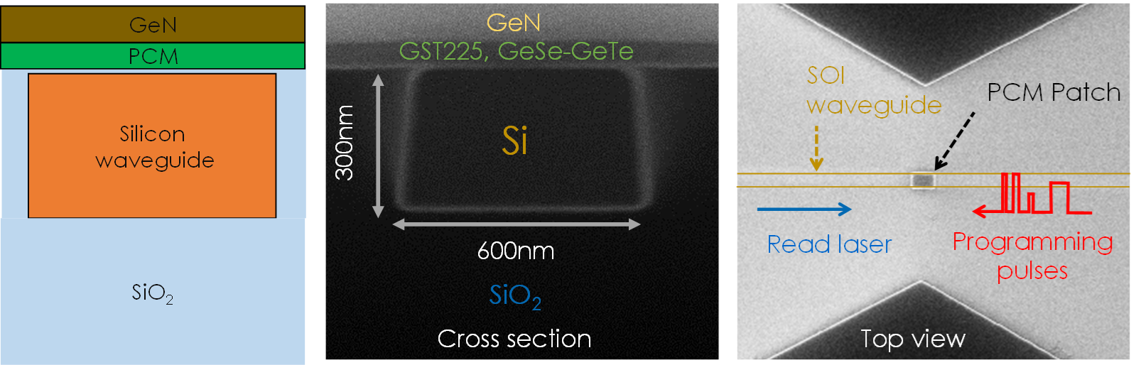
(Left) Schematic view of the stack of materials on top of the encapsulated silicon guide. (Middle) SEM FIB section of the profile of the resulting structure. (Right) Top view of the SOI guide decorated with the phase change material (PCM) patch.