Controlling optical properties at the nanoscale: an (electro-)chemical approach
Fedja Wendisch, Theresa Bartschmid, Joshua Piaskowski, Amin Farhadi, Gilles Bourret
Department of Chemistry and Physics of Materials, University of Salzburg, Austria
The intrinsic constraints of conventional synthetic and lithographic techniques have limited the types of heterostructures that can be created and studied in the laboratory. Here, I will review the use of bench-top templated electrochemical lithographies1-3 and metal-assisted chemical etching (MACE)4 for synthesizing a variety of complex metal/semiconductor heterostructures with spatial resolution down to the nanometer range. The preparation of nanostructure silicon arrays via MACE will be specifically discussed, together with the integration of defined metal nanostructures at the silicon surface using (electro-)chemical approaches.
Control over E-field enhancement and light absorption at the nanoscale will be discussed in the context of surface-enhanced Raman scattering, and photocatalysis.
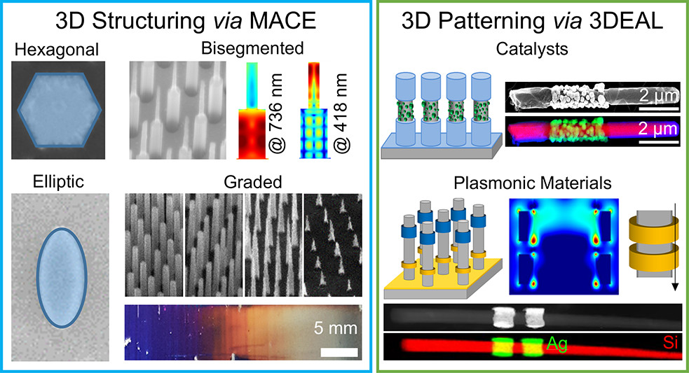
Engineering light absorption in three dimensions within silicon nanowire arrays using chemistry.
Reference
[1] T. Ozel, G. R. Bourret, and C. A. Mirkin Nature Nanotechnol. 2015, 10, 319
[2] F. J. Wendisch, M. S. Saller, A. Eadie, A. Reyer, M. Musso, M. Rey, N. Vogel, O. Diwald, G. R. Bourret Nano Lett. 2018, 18, 7343
[3] J. Piaskowski, G. Haberfehlner, T. Bartschmid, G. Kothleitner, M. Steinhart, G. R. Bourret J. Mater. Chem. C 2023, 11, 10872
[4] F. Wendisch, M. Rey, N. Vogel, G. R. Bourret Chem. Mater. 2020, 32, 9425.